Interesting Knowledge About PCB | PCB Assembly Line
30 July 04

Interesting Knowledge About PCB | PCB Assembly Line
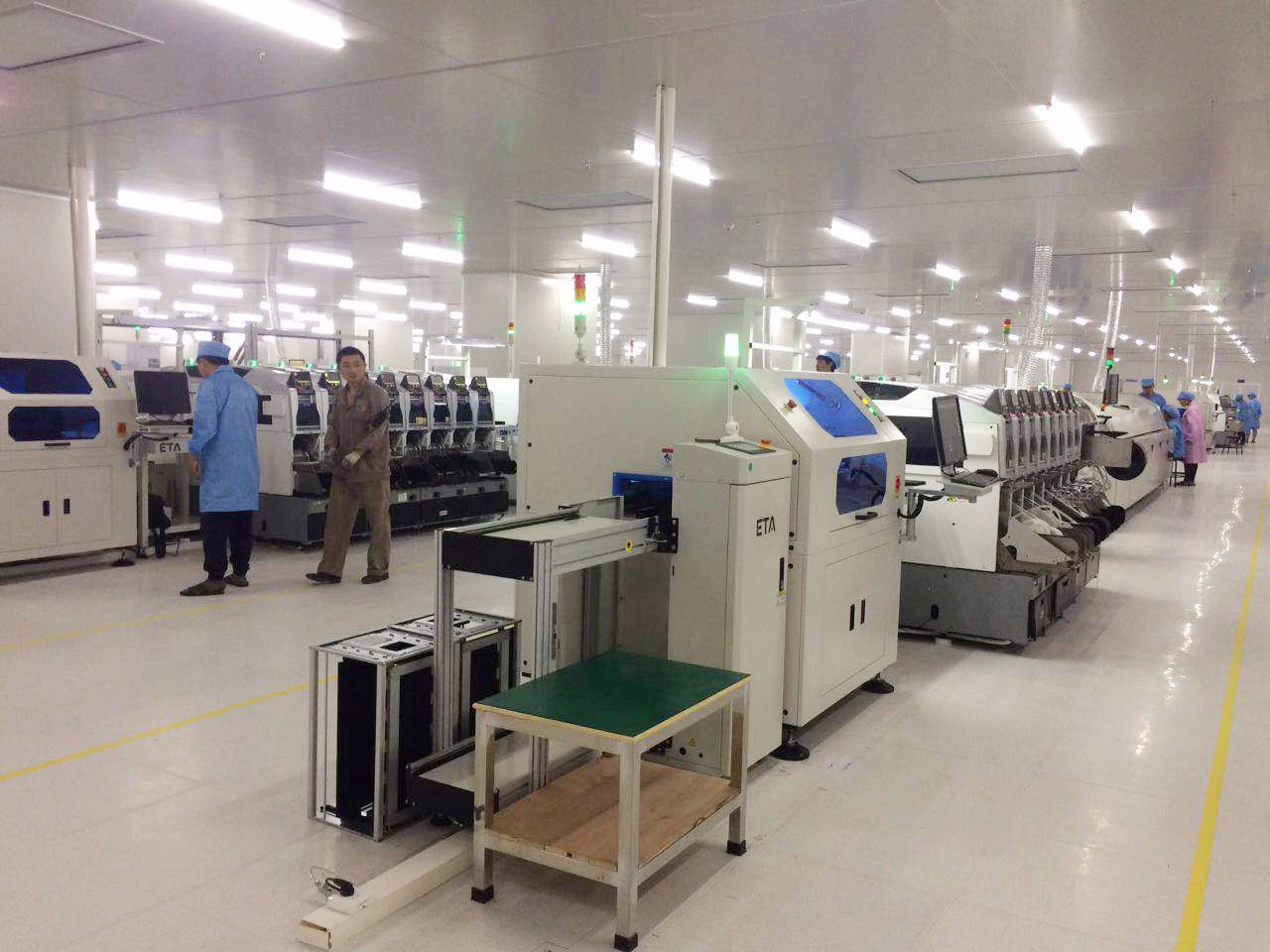
ETA provides high speed SMT production line, PCB assembly line, and turnkey SMT line , SMT solutions, for SMT smart factory.

There is no doubt that the printed circuit board (PCB) is a landmark tool in human technology.
PCB has become a means of optimizing the production process of electronic equipment. In the past, those hand-made electronic equipment had to be replaced by PCB. This is because more functions will be integrated on the circuit board.
Compare the circuit board in a calculator in 1968 with a modern computer motherboard

1.Color:
Even for some people who don't know what a PCB does, they generally know what a PCB looks like. They at least seem to have a traditional style, which is its green color. This green is actually the transparent color of the solder mask glass paint. Although the name of the solder mask is solder mask, its main function is to protect the covered circuit from moisture and dust.
As for why the solder mask is green, the main reason is that green is the military protection standard. The PCB in the military equipment first used the solder mask to protect the reliability of the circuit in the field. Green is the natural protection color in the military. Some people think that the color of the epoxy resin used in the original solder mask paint is green, so it is still used today.
Now the color of the solder mask is various, including black, red, yellow and so on. After all, green is not an industry standard.
2. Who is the first man invented the PCB?
The earliest printed circuit boards need to be traced to the Austrian engineer Charles Ducas in 1920, who proposed the concept of using ink to conduct electricity (printing brass wires on the bottom plate). He used electroplating technology to produce wires directly on the surface of the insulator, and produced a PCB prototype.
The metal wires on circuit boards were originally brass, an alloy of copper and zinc. This disruptive invention eliminates the complicated wiring process of electronic circuits and ensures the reliability of circuit performance. This process did not enter the practical application stage until the end of the Second World War.
3. Mark:
There are a lot of white marks on the green circuit boards. For many years, people did not understand why these white printed marks were called "silk screen layers." They are mainly used to identify the information of the components on the circuit board, and other content related to the circuit board. This information can help circuit engineers to check whether there are faults in the circuit board.
❙ PCB Assembly Line Video


